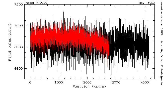
Flatfields
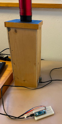
To generate flat field exposures I build a wooden box. The box is some 30 centimeters high and contains a back illuminated piece of white paper of 2.5 centimeters radius. Every pixel of the device on top has an unobstructed view onto this illuminated area. The illumination is done by some white LEDs whose brightness are controlled by an Arduino Micro microprocessor via a pwm output. The output runs at a frequency of 1 kHz and the on-time of the LED is a fraction of each period. The fraction is n/255. Where n is a number between off = 0 ≤ n ≤ 255 = full on. The number of photons send to the detector is shurely proportional to that number n. The exposure time was constantly 0.1 seconds. So 100 packages of photons will reach the detector chip in 0.1 seconds. Sometimes nearly 99, sometimes nearly 101.
The brightness in the box ranged from n=0 to n=250 in steps of 10. For every step I made 10 exposures and additional 25 darks, all of 0.1 s duration. The exposures of each step where mean averaged and master dark subtracted.
Here are the results of the test series.
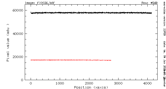
With the ASI you get 3.13 times more ADUs than with the Atik for the same number of photons. That's impressive. The flats of the ASI are also flatter than those of the Atik. And the snr of the flat made with the CMOS detector is better than that of CCD.
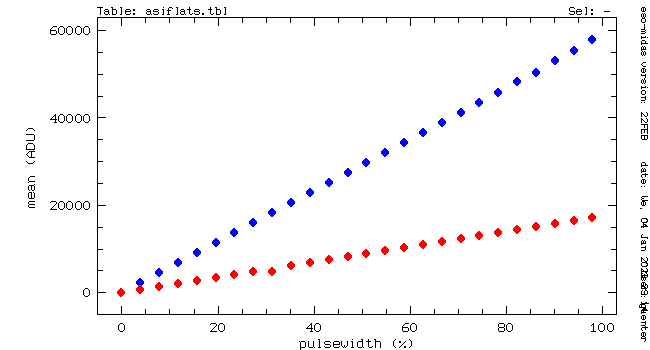
Do not trust the Atik value at 31% pulse width.
I forgot to enlarge the brightness.
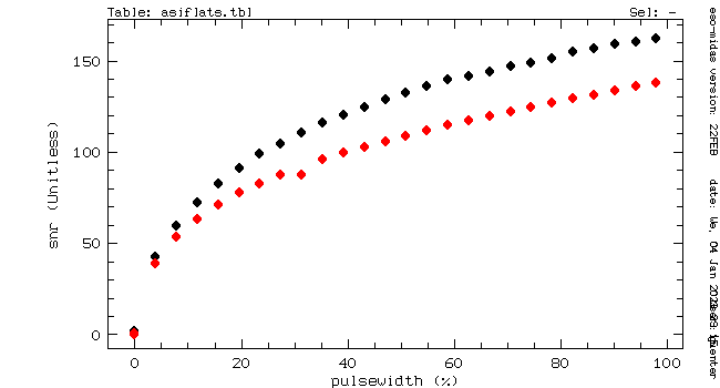
My conclusion is that the CMOS chip is slightly better than the CCD detector. See a more in depth discussion at Christian Buil's site and look for the CMED algorithm.
Last modified: 2023 Jan 13